
I have already posted a article on introduction to dspic microcontrollers. Today’s our subject will be about dsPIC30f2010 Microcontroller, where we discuss its basic introduction, feature and pin out as well.In it, the core always has 24 bit instructional word. PC (Program Counter) is 23 bits extensive with LSb (least significant bit) and the MSb (most significant bit) is always ignored during the normal running of program except for some certain conditions or instructions. Then the PC addresses up to 4M instructional words. There it uses an instructional mechanism just to maintain a throughput. Program loop uses the DO and REPEAT instructions. These both are interruptible at any point of program. 16 x 16 bit register act as data, address and offset register.When we talk about data space which is 64 Kbytes (32K words) and split into 2 blocks referred as X and Y data memory. Both of these blocks has its own Address Generation Unit (AGU).
There is a specification of X and Y in dsPIC30f2010 Microcontroller that these are device specific and could not be altered by their users. While overhead free circular buffer are supported in both X and Y address space.The core maintenance Inherent, Relative, Literal, Register Offset, Register Direct, Register Indirect, Literal Offset Addressing Modes. Most of the instructions are related to the predefined Addressing modes and depending upon their functional specifications.In most of the instructions, core is clever enough to run a program data memory read, a data memory write, and an instruction memory read per its instruction cycle.And core does not backing or support a multi-stage data pipeline but a single stage data prefetch mechanism is used here, which partially decodes instructions a cycle ahead of running, just to increase available running time. Most of the data/instructions run in a single cycle, with certain exceptions.
Programmer’s Model of dsPIC30f2010 Microcontroller mostly consists of 16 x 16 bit working registers. Some registers as like Status Register (SR), DO and REPEAT register, Program Space Visibility Page registers (PSVPAG), Data Table Page register (TBLPAG) and Program Counter (PC) act as address, data or offset registers. These all are memory mapped. Some of them has a shadow register with each of these registers. Actually the shadow register is used temporarily and these can move its data or contents from its host register on the occurrence of an event. But there is a specific condition occurs that shadow register could not access directly. At working register when a byte operation is performed, at that time just the Least Significant Byte (LSB) of the specific register is affected.
In dsPIC DSC devices, SOFTWARE STACK POINTER or FRAME POINTER are used. W15 is software Stack Pointer (SP), which has the ability to modify automatically by processing , calls and returns. However, W15 could be referenced through any order but in the same manner as like all other W registers. It simplifies the reading, writing and many other manipulations of the Stack Pointer. During a Reset ,W15 is initialized to 0x0800. You may reprogram the SP (Stack Pointer) during initialization to any position within data space. W14 register has been devoted as a Stack Frame Pointer (SP) as defined by the ULNK and LNK instructions.
Table of Contents
Pin Layout of Dspic30f2010
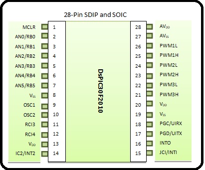
| PIN # (n) | PIN NAME + DESCRIPTION | Port |
| 1 | MCLR | Master Clear (Reset) input or programming voltage input. |
| 2 | EMUD3/AN0/VREF+/CN2/RB0 | B |
| 3 | EMUC3/AN1/VREF-/CN3/RB1 | B |
| 4 | AN2/SS1/CN4/RB2 | B |
| 5 | AN3/INDX/CN6/RB3 | B |
| 6 | AN4/QEA/IC7/CN6/RB4 | B |
| 7 | AN5/QEB/IC8/CN7/RB5 | B |
| 8 | Vss | Ground reference for analogue module |
| 9 | OSC1/CLKI | Oscillator Input |
| 10 | OSC2/CLKO/RC15 | Oscillator |
| 11 | EMUD1/SOSCI/T2CK/U1ATX/CN1/RC13 | C |
| 12 | EMUC1/SOSCO/T1CK/U1ARX/CN0/RC14 | C |
| 13 | RC2/CCP1/VDD1A | C |
| 14 | EMUD2/OSC2/IC2/INT2/RD1 | D |
| 15 | EMUC2/OC1/IC1/INT1/RD0 | D |
| 16 | FLTA/INT0/SCK1/OCFA/RE8 | E |
| 17 | PGD/EMUD/U1TX/SDO1/SCL/RF3 | F |
| 18 | PGC/EMUC/U1RX/SDI1/SDA/RF2 | F |
| 19 | Vss | Ground |
| 20 | VDD | Positive Power Supply for analogue module |
| 21 | PWM3H/RE5 | E |
| 22 | PWM3L/RE4 | E |
| 23 | PWM2H/RE3 | E |
| 24 | PWM2L/RE2 | E |
| 25 | PWM1H/RE1 | E |
| 26 | PWM1L/RE0 | E |
| 27 | AVSS | Analogue Ground |
| 28 | AVDD | Analogue Power Supply |
Features
Now let us discuss the features of dsPIC30F2010 separately.
High-Performance Modified RISC CPU:
- It has Modified Harvard Architecture
- 84 base directions with flexible tending to modes
- C compiler optimized instruction set of design
- 27 intersect sources
- 3 external interrupt sources
- 24-bit wide guidelines, 16-bit wide data way
- 16 x 16-bit working register cluster
- Up to 30 MIPs task:
- DC to 40 MHz outer clock input
- 4 MHz-10 MHz oscillator contribution with PLL active (4x, 8x, 16x)
- Peripheral and External interface with sources
- 8 user selectable need levels for each hinder
- 4 processor exemptions and programming traps
- Primary and Alternate interface with Vector Tables
DSP Engine Features
- Modulo and Bit-Reversed Addressing modes
-
-
- Two, 40-bit wide aggregators with discretionary saturation logic
- 17-bit x 17-bit single cycle equipment fragmentary/whole number multiplier
-
- Single cycle Multiply-Accumulate (MAC) task
- Dual information fetch
- 40-organize Barrel Shifter
Peripheral Features:
- High current source/sink I/O pins: 25 mA/25 mA
- Optionally combine up 16-bit timers into 32-bit clock modules
- 3-wire SPI™ modules (underpins 4 Frame modes)
- I2C™ module bolsters Multi-Master/Slave mode and 7-bit/10-bit addressing
- There addressable UART modules with FIFO buffers
Motor Control PWM Module Features:
- Complementary or Independent Output modes
- Edge and Center Aligned modes
- Multiple obligation cycle generators
- Dedicated time base with 4 modes
- Programmable yield polarity
- Dead time control for Complementary mode
- Manual yield control
- Trigger for synchronized A/D transformations
Quadrature Encoder Interface Module Features:
- Phase A, Phase B and Index Pulse input
- 16-bit up/down position counter
- Count bearing status
- Position Measurement (x2 and x4) mode
- Programmable digital noise filters on contributions (inputs)
- Alternate 16-bit Timer/Counter mode
- Interrupt on position counter rollover
Analog Features:
- 10-bit 1 Msps Analog-to-Digital Converter (A/D)
- A/D Conversion accessible amid Sleep and Idle
- 4 Sample/Hold Channels
- Multiple Conversion Sequencing Options
Special Microcontroller Features:
- Improved Flash program memory:
- 10,000 delete/write cycle (min.) for industrial temperature range, 100K (typical)
- Data EEPROM memory:
- 100,000 delete/write cycle (min.) for industrial temperature range, 1M (typical)
- Self-re programmable under software control
- Power up Timer (PWRT), Power on Reset (POR) and Oscillator Start-up Timer (OST)
- Flexible Watchdog Timer (WDT) with on-chip low power RC oscillator is used for reliable operation
- Fail-Safe clock screen / monitor task
- Detects clock catastrophe and switches to on-chip low power RC oscillator
- Programmable code assurance
- In-Circuit Serial Programming™ (ICSP™)
- Programmable Brown-out Detection and Reset generation
- Selectable Power Management modes
- Idle, sleep and Alternate Clock modes
CMOS Technology:
- High speed Flash machinery with low power
- Wide operating voltage range (2.5V to 5.5V)
- Industrial and Extended temperature ranges
- Low power utilization