
USE INPUT OUTPUT PORTS OF PIC18F452 MICROCONTROLLER: PIC18F452 microcontroller has a number of input/output pins which are used for connection with external devices. It has total 40 pins. Out of these 40 pins, 34 pins can be used as input output pins.These pins are grouped into five which are called PORTS denoted by A, B, C, D and E. Here in this article we will learn how to use I/O Ports of PIC18F452.
- Port A consists of seven pins named as RA0-RA6
- Port B consists of eight pins named as RB0-RA7
- Port C consists of eight pins named as RC0-RC7
- Port D consists of eight pins named as RD0-RD7
- Port E consists of three pins named as RE0-RE2
Some pins of the I/O ports are multiplexed with an alternate function from the peripheral features on the device. If a pin is used as any other function then it may not be used as a general purpose I/O pin. Here we will just restrict with the input output features of ports.
REGISTERS:
Each port has three registers for its operation. These registers are
• TRIS register (data direction register)
• PORT register (reads the levels on the pins of the device)
• LAT register (output latch)
- TRIS REGISTER:
TRIS is a data direction register. Setting TRIS bit for corresponding port will let know the data direction (whether read or write) to microcontroller. Each PORT has its own TRIS register E.g: For PORT A
TRISA=0 //making port as output port (write)
TRISA=1 //making port as input port (read)
We can also make specific bits of port as input or output.
TRISA.F2 = 1; // PORTA pin RA2 configured as input
- PORT REGISTER:
It reads the levels on the pins of the deviceand it assigns logic values (0/1) to the ports.The role of the PORT register is to receive the information from an external source (like a sensor) or to send information to the external elements (like an LCD). E.g:
For input mode of PORT A
Reading the PORTA register reads the status of the pins. We will firstly set the direction of data by TRIS register TRISA bit=1. It will make the corresponding PORTA pin an input and put the corresponding output driver in a Hi-Impedance mode.
TRISA=1 //making port as input port (read)
PORTA=0x** //Assigning low logic to the pins by external circuitry or device (Push button)
For output mode of PORT A
We will first set the direction of data by TRIS register. Then port is given the value for output. A write to the PORT register writes the data value to the port latch.
TRISA=0 //making port as output port (write)
PORTA=0x03; //Assigning high logic to the RA0 and RA1
- LAT REGISTER:
The Data Latch register is also memory mapped. LAT register is associated with an I/O pin. It eliminates the problems that could occur with read-modify-write instructions.
Latch Read:
A read of the LAT register returns the values held in the port output latches, instead of the values on the I/O pins. A read-modify-write operation on the LAT register which is associated with an I/O port, avoids the possibility of writing the input pin values into the port latches.
Latch Write:
A write to the LAT register has the same effect as a write to the PORT register. A write to the PORT register writes the data value to the port latch. Similarly, a write to the LAT register writes the data value to the port latch.
PORT A:
PORTA is a 7-bit wide, bi-directional (I/O) port. The corresponding Data Direction register is TRISA. This Port contains various features mentioned below:
- Port A pins are also multiplexed with analog inputs, i.e RA0, RA1, RA2, RA3, RA5 have AN0, AN1, AN2, AN3, AN4 respectively.
- The RA4 pin is multiplexed with the Timer0 module clock input to become the RA4/T0CKI pin. This pin is a Schmitt Trigger input and an open drain output.
- All other PORTA pins except RA4 have TTL input levels and full CMOS output drivers.
- RA2 and RA3 are also multiplexed with the analog VREF- and VREF+ inputs.
- RA5 also act as slave select input for synchronous serial port and can be used as low voltages detect input.
- RA6 is used as OSC2 or clock pin.
The operation of each pin is selected by setting the control bits in the ADCON1 register.
| Bit0 RA0 | I/O | AN0 | TTL | ||||
| Bit1 RA1 | I/O | AN1 | TTL | ||||
| Bit2 RA2 | I/O | AN2 | TTL | VREF- | |||
| Bit3 RA3 | I/O | AN3 | TTL | VREF+ | |||
| Bit4 RA4 | I/O | T0CKI | ST | ||||
| Bit5 RA5 | I/O | AN4 | TTL | SS,LVDIN | |||
| Bit6 RA6 | I/O | TTL | OSC2/CLK0 |
PORT B:
PORTB is an 8-bit wide, bi-directional port. The corresponding Data Direction register is TRISB.
- AllPORTB pins have a weak internal pull-up. A single control bit (clearing bit RBPU) can turn on all the pull-ups. For port pin as output, this weak pull-up is automatically turned off. The pull-ups are disabled on a Power-on Reset.
- Four of the PORTB pins, RB7:RB4, have an interrupton-change feature. The pins which are configured as inputs can only cause this interrupt to occur. This interrupt can wake the device from SLEEP.
- RB0, RB1 and RB2 can be used as external interrupt inputs.
- RB3 can be used as the alternate peripheral pin for the CCP2 module.
| Bit0 RB0 | I/O | TTL/ST | INT0 | |||
| Bit1 RB1 | I/O | TTL/ST | INT1 | |||
| Bit2 RB2 | I/O | TTL/ST | INT2 | |||
| Bit3 RB3 | I/O | TTL/ST | CCP2 | |||
| Bit4 RB4 | I/O | TTL | Interrupt on change | |||
| Bit5 RB5 | I/O | TTL/ST | Interrupt on change | ICSP enable pin | ||
| Bit6 RB6 | I/O | TTL/ST | Interrupt on change | Serial prog. clock | ||
| Bit7 RB7 | I/O | TTL/ST | Interrupt on change | Serial prog. data |
PORT C:
PORTC is an 8-bit wide, bi-directional port. The corresponding Data Direction register is TRISC. PORTC is multiplexed with several peripheral functions:
- PORTC all pins have Schmitt Trigger input buffers.
- RC1 is configured as the default peripheral pin of the CCP2 module and RC2 for CCP1.
- RC4 can also be the SPI Data In (SPI mode) or Data I/O (I2C mode).
- RC5 used for Synchronous Serial Port data output SDO
- RC6 is used as Addressable USART Asynchronous Transmit, or Addressable USART Synchronous Clock.
- RC7 is used as Addressable USART Asynchronous Receive, or Addressable USART Synchronous Data.
| Bit0 RC0 | I/O | ST | TMR1 oscillator output | |||
| Bit1 RC1 | I/O | ST | TMR1 oscillator input | CCP2 | ||
| Bit2 RC2 | I/O | ST | CCP1 | |||
| Bit3 RC3 | I/O | ST | ||||
| Bit4 RC4 | I/O | ST | SDI/SDA | |||
| Bit5 RC5 | I/O | ST | SDO | |||
| Bit6 RC6 | I/O | ST | TX/CK | |||
| Bit7 RC7 | I/O | ST | RX/DT |
PORT D:
PORTD is an 8-bit wide, bidirectional port. The corresponding Data Direction register is TRISD.
- PORTD all pins have Schmitt Trigger buffers when in I/O mode.
- It can be configured as a parallel slave port by setting control bit PSPMODE (TRISE<4>). In this mode, the input buffers are TTL.
| Bit0 RD0 | I/O | ST/TTL | parallel slave port bit0 |
| Bit1 RD1 | I/O | ST/TTL | parallel slave port bit1 |
| Bit2 RD2 | I/O | ST/TTL | parallel slave port bit2 |
| Bit3 RD3 | I/O | ST/TTL | parallel slave port bit3 |
| Bit4 RD4 | I/O | ST/TTL | parallel slave port bit4 |
| Bit5 RD5 | I/O | ST/TTL | parallel slave port bit5 |
| Bit6 RD6 | I/O | ST/TTL | parallel slave port bit6 |
| Bit7 RD7 | I/O | ST/TTL | parallel slave port bit7 |
PORT E:
PORTE is a 3-bit wide, bi-directional port. The corresponding Data Direction register is TRISE.
- These pins have Schmitt Trigger input buffers.
- They also control the parallel slave port operation.
- PORTE pins are multiplexed with analog inputs. When using them as analog inputsthey must be configured as inputs.
| Bit0 RE0 | I/O | AN5 | ST/TTL | RD | parallel slave port bit0 |
| Bit1 RE1 | I/O | AN6 | ST/TTL | WR | parallel slave port bit1 |
| Bit2 RE2 | I/O | AN7 | ST/TTL | CS | parallel slave port bit2 |
EXAMPLE:
PROTEUS SIMULATIONS:
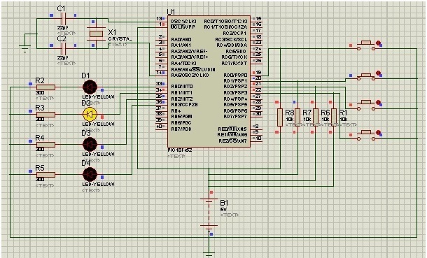
WORKING:
PIC18F452 PORT B pins are configured as output and PORT D pins are configured as input. We have used 4 push buttons. Crystal of 12MHz can be used. All LED are firstly turned off.
Coding is done as:
- If 1st button is pressed then 1st LED will glow for onesecond and then turn off.
- If 2nd button pressed, 2nd LED will glow for onesecond and then turn off and so on…
- Whenever Button is pressed, corresponding LED will glow.
- In short we are reading data from PORT D and writing data to PORT B.
CODE:
void main()

{

  TRISD.F0 = 1;                    //Configure 1st bit of PORTD as input

  TRISD.F1 = 1;                    //Configure 2nd bit of PORTD as input

  TRISD.F2 = 1;

  TRISD.F3 = 1;

  TRISB.F0 = 0;                    //Configure 1st bit of PORTB as output

  TRISB.F1 = 0;                    //Configure 2nd  bit of PORTB as output

  TRISB.F2 = 0;

  TRISB.F3 = 0;


  PORTB=0x00;                   //All LEDs OFF

do

  {

if(PORTD.F0 == 0)            //If 1st switch is pressed

    {

         PORTB.F0 = 1;           //1st LED ON

Delay_ms(1000);              //1 Second Delay

         PORTB.F0 = 0;           //LED OFF

    }


if(PORTD.F1 == 0)            //If the 2nd switch is pressed

    {

         PORTB.F1 = 1;           //2nd LED ON

Delay_ms(1000);              //1 Second Delay

         PORTB.F1 = 0;           //LED OFF

    }


if(PORTD.F2 == 0)            //If the 3rd switch is pressed

    {

         PORTB.F2 = 1;           //3rd LED ON

Delay_ms(1000);              //1 Second Delay

         PORTB.F2 = 0;           //LED OFF

    }

if(PORTD.F3 == 0)            //If 4th switch is pressed

    {

         PORTB.F3 = 1;           //4thLED ON

Delay_ms(1000);              //1 Second Delay

         PORTB.F3 = 0;           //LED OFF

    }


}

while(1);

}