
Table of Contents
Introduction to watchdog Timer
In this article we will see how to use watchdog timer and sleep mode of pic microcontroller. The watchdog timer is actually the type of free running on chip RC oscillator, that does not require any other external components for their operation. The pin OSC1/CKLIN of RC oscillator device is basically separate from RC oscillator, this means that the WDT will run continuously even when the pins OSC2 and OSC2 is stopping, supposed by executing the sleep instruction. The device configuration bit can enable or disable the watch dog timer and the software execution cannot be disabled the function if the function is enabled by the watchdog timer.The block diagram of watchdog timer is shown in figure.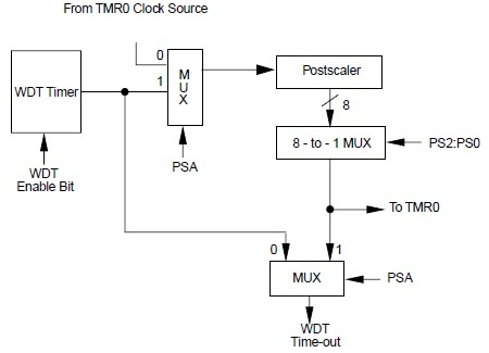
Figure 1 The Block Diagram of Watchdog Timer
Watchdog Timer Control Registers
The watchdog timer consists of several type of control registers such as OPTION_REG, that contains different types of configure and control bits’ like TMR0 pre scaler or WDT post scaler, INT the external interrupt, TMR0 and weak pulls up on PORT B. All the bits are readable and writable. The watchdog timer with all the register and controls bits is shown below.
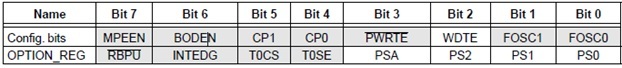
Bit 7: The RBPU is weak pull up enable bit, the digit 1 is used for disable the weak pull up and the digit 0 is used for disable the weak pull up. These are the latch values of individual port.
Bit 6: INTEDG, which is the interrupt edge select bit, the digit 1 is used for rising edge of INT pin and digit the 0 is used for falling edge of INT pin
Bit5:T0CS, which is clock source select bit, the digit 1 is used for transition on T0CKI pin and the digit 0 is used for selecting the internal instruction clock cycle.
Bit 4: TOSE, which is source edge select bit, the digit 1 is used for incremental transition high to low on T0CKI pin and the digit 0 is used for incremental transition low to high on T0CKI pin.
Bit 3: PSA, which is pre scale assignment bit, the digit 1 is used for assign the pre scaler value to WDT and the digit 0 is used for assign the pre scaler value to timer 0.
Bit 2: PS2, PS0 these are the pre scalar and post scaler rates of watchdog timer to select the bit. Shown in table 1
Table 1 Watchdog Timer Rates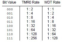
Operation of Watchdog Timer
When the device is in normal operating condition then, the watchdog timer (WTD) just RESET the device, similarly, when the device is in sleep mode then it just wake up the device so that it operate continuously in normal operating condition and this wake up is called watchdog timer wake up. By clearing the configure bit WDTE, the watchdog timer can be permanently disabled.
The pre and post scaler assignments are fully controlled by the software therefor, it can be only changed during the program execution. In order to avoid the RESET of device, unintentionally the watchdog timer changing pre scaler instruction (Timer0 to WDT) must be executed even when the watchdog timer is disabled.
frequency of WDT
The optimum time out period of watchdog timer is 18 ms, but it is without post scaler. This time period also changes with VDD, variation in process from part to part and variation in temperature. If the long time is required for adequate output, then the watchdog timer can assign the time division ratio up to 1:128 to the post scaler. This can be done through the software control by writing in register OPTION_REG.The time out period can be realized up to 2. 3 sec.
For clearing the watchdog timer and post scaler the instructions SLEEP and SLRWDT are used. These instructions also prevent the device to time out and RESET the device. This should be always kept in your mind under worst condition if VDD is minimum, Temperature is maximum and watchdog timer post scaler is maximum then the device would be take several seconds before the WTD time out occur.
SLEEP MODE or Power Down Mode
The sleep mode is the mode when there is nothing take place in other words, the device is in rest mode, because the device is nothing doing therefore, in this mode power consumption would be lowest and the oscillator would be tuned off. For entertained this mode the SLEEP instruction is used. When it is enabled the watchdog timer and PD bit in status register would be both cleared, but WTD keeps on running. The TO bit sets and oscillator is tuned off. The Inputs and outputs pins keeps the status on before they have.
In this mode because there is lowest current consumption therefore all the inputs and outputs pins would be either at VDD or VSS, no current is drawing by the external circuitry and the module which have delta sleep current is also disabled
Wake UP from Sleep Mode
The device which have the watchdog timer is wake up one of following bellow conditions.
- When any device is reset.
- When enabled the watchdog timer.
When any relating module is set as an interrupt during the sleeping mode such as, External input PIN, Change the port pin, Comparator, A/D, Timer, LCD, SSP and Capture. When any condition is set up then then watchdog timer is waked up. Once the watchdog time is wake up then it resumes the program execution. The TO and PD bits of status register can be used for the knowing the reason of wake up of device or reset.
The PD bit is cleared which the device is set up in reset mode form power up mode and the watchdog timer is wake up when the TO bits is cleared. When the device is wake up then the next instruction automatically comes up in operation. When the device is wake up through an external event interrupt then the cross ponding bit must be enable. During the device the wake up then there would be no effect on GIE bit. When the GIE bit is enable then the device executes that instruction which come after the sleep instruction.
Wake up from sleep mode by Using Interrupts
When the interrupt is occurred before the execution of SLEEP instruction then the WDT and WDT post scaler will not be cleared. The TO and PD bits are also not cleared. When the interrupt is occurred after the SLEEP instruction then the device wake up immediately from sleep mode and the SLEEP instruction completely executed. During this condition the WTD and WTD post scaler will be cleared.
Applications of Watchdog Timer Mode
- This timer is used in that applications where the user continuously set and reset the operating system when it is in running condition.
- The primary application of watchdog timer is to monitor the system to detect and set the control system of microprocessor.
- When the code in microcontroller is not properly executing then the watchdog timer reset the microcontroller for proper execution of this code.